Reverse engineering Jane Street's ASIC puzzle
2026-09-05 · Code on GitHub
Approach to solution
My raw notes for this puzzle: rawNotes.pdf
For this puzzle, I used a combination of three analyses to solve it. By solving the puzzle, I mean finding the correct 121-bit signal required, but ALSO understanding how the circuit functions at a logic gate level. First, I will go through the GDS parsing (link to topic on that), then the circuit analysis I did mostly from step 5 of the GDS parser, under the Cones, and finally using Z3 to understand the data path combinational blocks, as well as looking into what 121-bit signal sets the success signal high. IMPORTANT Note: I want this write-up to focus much more on the circuit analysis and less on the scripting, although it was what provided the solution that involved using external complex computing algorithms and a lot of Claude Code. The scripts helped me make some jumps in the circuit analysis that would have taken significantly longer if I were only doing the circuit analysis.
GDS Parsing
From a broad standpoint, the GDS parsing was a 5-stage process, starting from the .gds file to a formatted GDS file, to a graph of all cells to a graph of logical cells connected(netlist), to a graph of nodes of combinational blocks and edges being D-flip-flops. For this task, I used a lot of vibe coding but kept this pipeline as the underlying idea.
Python Scripts from GDS to winning solution
GDS file to netlist graph
The first file to look into is klayoutNetlist. This really does the first 3 steps of the pipeline described above, taking a GDS file as an input and a netlist as an output. To simplify this step as much as possible, I asked Claude to also use the Klayout LayoutToNetlist tool for this task. What this provided was a readable file in return that the Python file organizes into formatted information. The information important are instances of cells; this is a graph of sky130 logic cells as nodes and connections between each as edges. So this step allowed us to take a GDS file, which does not have a user-readable format and turn it into a data structure that is very easy to walk through and understand for later algorithms created.
Netlist to Combinational Blocks
So now there is a Netlist Graph, the issue with a netlist graph is the size and organization; the amount of cells is too large to say draw out and if you tried making specific larger blocks from this step you would have to think of some algorithm that says there is a limit to how many logic cells I will search around me before I am just making the entire circuit in this clock. Instead, for organization, we can just separate the chip's design into every combinational block between two flip-flops. What this gives us is an organized set of every computational step in this circuit AND a very definitive approach to achieving this organized set; all you are doing is walking some graph to see all cells between a data input pin of a flip-flop to the output of another flip-flop or a direct input of the circuit. For this step, I used coneDecompose.py, which, as stated before, just starts walking back from every sequential element to the FF outputs and chip inputs to provide the fan-in of the cone.
JSON Files to Verilog
With two data structures containing the recovered GDS file, the next step is turning these into Verilog files to test if the algorithms Claude created actually worked. This is when coneToVerilog.py and netlistVerilog.py are used. All it does is parse a JSON file, and it does so in two main functions: cleaning the JSON file to include only the specific information the parser needs and then declaring ports, which provide the name and direction of each port.
Now that I had a netlist and cones file to verify functionality, I made tb_cones.cpp and tb_netlist.cpp. I used a semi-UVM type of testbench made in C++ to test functionality. The hardest part of the testbenches was finding an efficient way to get the waveform data from example inputs into the C++ file, or into some format I could adjust easily to test. I had Claude create VCD parsing files and then, at some point, just had it put the characters directly in the C++ file so I could easily adjust. After some verification from the testbenches, we now had working Verilog files to do the circuit analysis.
Circuit Analysis
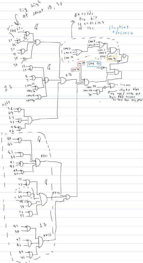
For the circuit analysis, I started by looking into the most complex cone. From looking at the Verilog file, CONE98 is the one to look into. It drives the success output, which is the function of the circuit, along with the output drivers. From here, I drew out this cone, as you can see below. When looking into this cone, I started by examining the cones based on how much influence they have on driving success.
Control
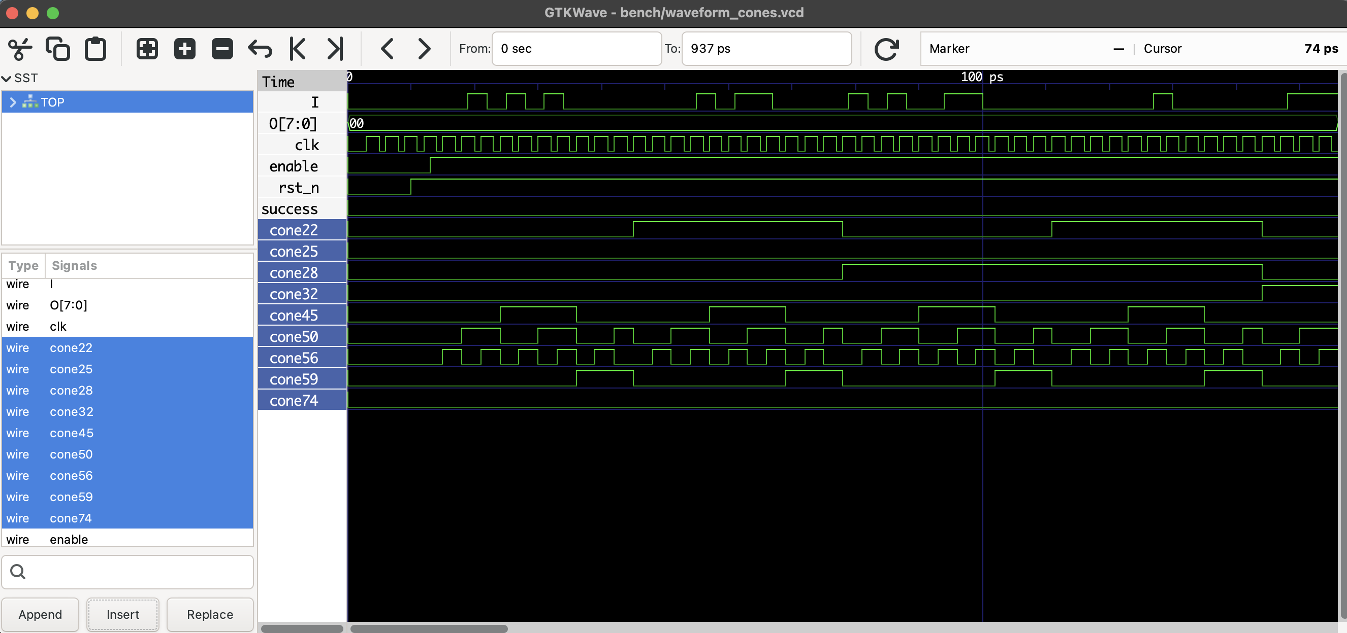
The first place this analysis took me was CONE74, which is a pin present in almost every pin. Now, its role in every pin is as a pair to the enable pin, meaning cones are not enabled when CONE74 is high, which occurs when the ASCII readout is happening. First thought when seeing the waveform is that CONE74 is the DONE state of the state machine. So if this is the state machine, I should see how the pins connected to it operate. After doing more analysis by drawing out the cones in my notes and viewing waveforms, I had the description of all state machine inputs, which were simply different modulo counters ranging from modulo-1, which just indexes on the rising edge of the clock, to modulo 44 for cone 32. The key things to pick up from the wave analysis I show below are the sequences like cone 45 and 59, which don't follow standard modulo but rather repeat every 11 clock cycles. This piece of evidence tells us the control is checking something, and the fact that it has checkers repeating every 11 clock cycles and it's a 121 clock sequence hints toward the 11x11 grid that is the final solution.
Bit counting
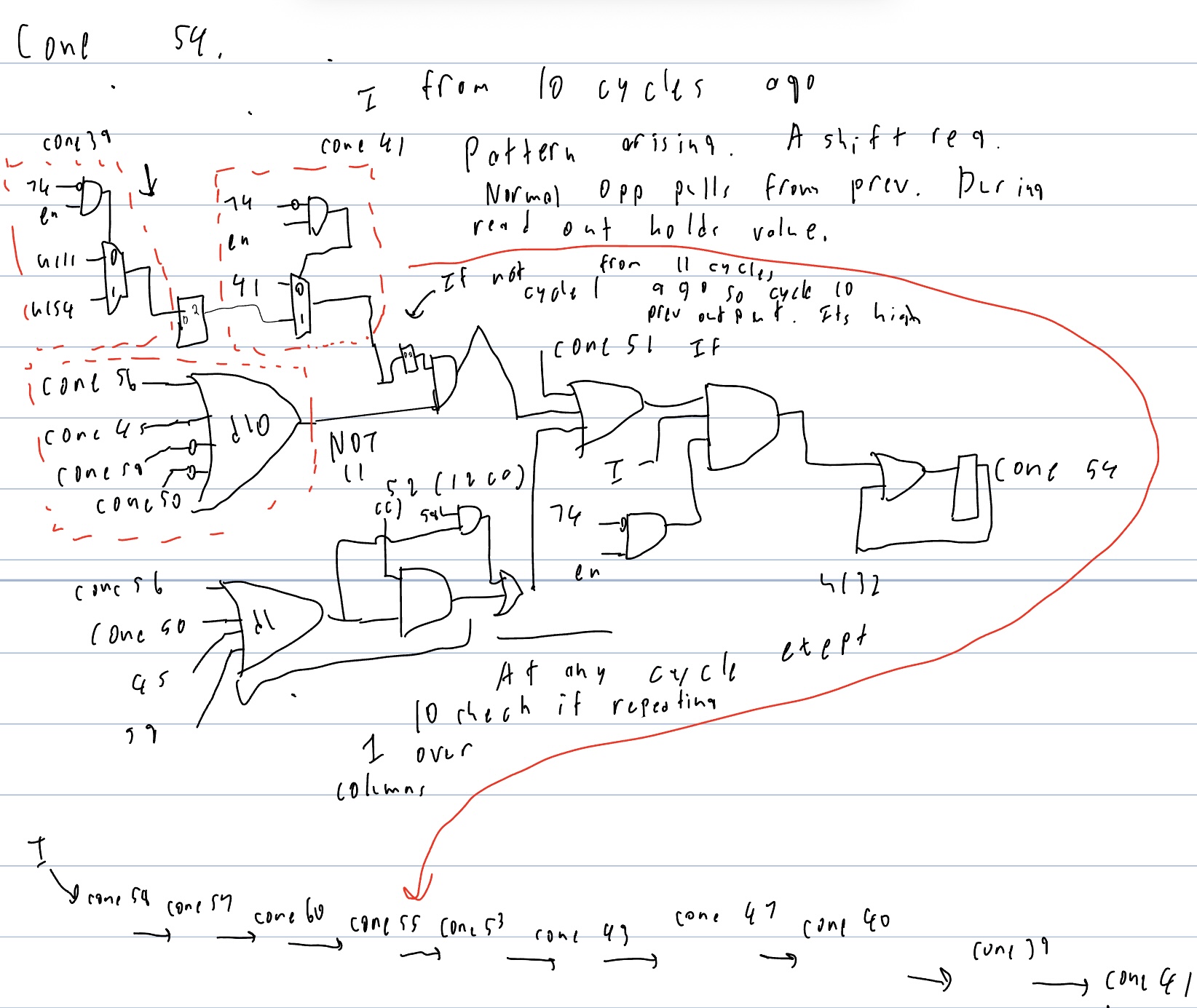
So, just from looking at cone 74, I found the functions of 10 cones. The next two areas were cone54 and the combinational block right beside cone 54 in the success cone. So cone 54 is a large combinational cone; control inputs stated above, along with inputs from cone 52, 58 and 41. When you look into those 3 cones, they are a shift register of every I input for the last 12 inputs. The exact structure is on page 6 of the notes but boils down to two control gates that go low at counts 1 and 11 of every signal, and three inputs from the register from I 1, 10, 11 and 12 clock cycles ago. We also know this is a sticky cone, and it must stay low to trigger success. After looking at the waveform, knowing the circuit and providing some sample inputs, we can see that this is test adjacency. The reason for the two control gates that go low at 11 and 1 was for a wrap-around from bit 11 of one sequence to bit one of the next; this should not set a flag. It is testing if two ones are ever diagonal or touching, and if so, success will not trigger. This is the first major hint into how to trigger success. The next analysis went into the cones directly beside it: cones 24, 1, 6, 3, 4 and 10. Cone 24, which holds the most significance, was a very simple circuit. When you derive circuits 26 and 31, you see that this is just counting two high bits and resets at count 11, simple as that, but it gives us another massive clue to find the solution. After seeing how cones 24,26 and 31 responded to inputs, I moved my analysis much more to checking waveforms. This gave me information on all other cones in that combinational block, and descriptions are in the notes. The summary is that each cone represents a count of high signals, and only a specific bit count turns this signal high: 22. So from this information, we have found that there are 22 bits, two high bits per 11 total bits, and they cannot be adjacent in any direction. That already gives you a lot of information about how the bit stream that drives success high will work.
Bit Checking with Control
So, from just analyzing 36 of the 99 cones in the ASIC, I know there are 22 ones in the solution, two per row, where a row is 11 bits, and the 1s can never touch if we imagine an 11x11 grid setup. Looking at what's left of the cone 98 structure, it is pretty obvious that the sea of AND gates probably links to sticky registers that go high when a specific part of the sequence happens. Now there are two approaches I took with trying to understand these, but a major disclaimer I want to note is that by this point I already knew the solution and making some of these leaps having zero clue what the solution looks like is much harder and not what I did; this is purely trying to understand how the circuit functions. Now the first idea you could use to derive this is knowing how the cones react to I. I will use an example for this: We want to know what triggers cone 30 to be low and cone 34 to be high. The first step is a 121-bit signal of all 1's this tells us how the cone reacts to these ones: will it do nothing, will it oscillate, or, in our case, cone 30 will go high at some specific moment and then drop right after. So we already know that cone 30 needs to go high, but we want 30 low and 34 high, which we are going to assume happens because of 30 already being high. So we erase all 1s before the 1 that triggers 30 and then have a zero after for every signal below for adjacency and try again. We see the cone 30 goes low at the next 1 in the same column. So that tells us that 30 is triggered by 1s in column 1, and from some other investigation we know it can trigger in any of the next columns(!!!). Now, the example I gave does have a lot of advantages because I have already found a valid sequence for success, but taking those debugging steps is possible and is how I was able to decode what the cones do. The cone analysis, however, changed for this. I used a tool with Z3 to provide all possible signals that can drive a cone to 0 or 1. I wanted to mention this for this step because it is another approach you could use to decode these blocks, and it does require lots of large jumps, as I took with the example, knowing there is going to be 1 bit after the bit that triggers cone 30 to trigger cone 34 and untrigger 30. This just requires knowing the bit count and control logic. If you put cone 34, the cone we want high from the previous example, into this Python file, it will output all possible combinations. Now it would be nice if it output one 11-bit sequence that worked, but instead there are several that work; for our knowledge of how the signals around work, you can narrow it down pretty quickly. One of which is that cone 30 must be high and I must be high, so the next place to look is how cone 34 gets high. This actually has a more decisive logic block but still has lots of combinations; the one thing to look at, however, is a specific combination. So I chose one where cone 25 was high and cone 50 as well, but every other clock was low. These are control blocks based solely on timing, so what this combination is giving me is a specific time point where, if I is high, then cone 34 will go high. If you use this combination with the test bench, you take your already narrow option of inputs and can narrow it down. Now I won't go too much into detail because I have spent a long time talking about the underlying mechanics of the circuit but if you test this for every group of two cones you see in the original schematic you get the pairs of mostly coloums checking if both bits are present but there are 6 cones; 93,94,96,97,99 and 101 where this doesn't happen and instead for example it will check the 1 bit in column 6 of row 2 and then go to bit columns 5 of row 7 it still checks all bits but does the check oddly. The lower group of cones check bits just by column in the standard way. 22 cones are dedicated to a change in how 3 columns of bits are checked, which I think is the complexity of the ASIC I just never got to.
(!!!)IMPORTANT: This description of cone 30 is wrong it functions differentely what this example explains is cone 66 and 64 where it will only be triggered by the specific 1's in the correct column and row.
Output buffers
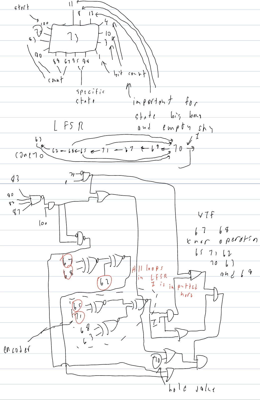
So by this point, about 80 cones' functionality has been discovered, specifically all cones that had some sort of direct wiring in the success block. What's left? The output generator, probably the most complicated part of the circuit, because how this occurs isn't as clear as the Bit checking with the control or success block. So where I start with this was cones that feed into the output block; start with as little logic as possible; this explained cones. What we have as inputs are really four main things: a 4-bit incrementing clock, the counter for how many 1's, cone to success and symmetric fan-in cone to it, cone 100, which is the signal to start write out and lastly cone 70. Cone 70 is an LFSR for every new input. My derivation for this was mostly based on the blocks around and the randomness you see. It is a combinational clock with the 4-bit clock, yet it runs through the operation, and it has chains of XNOR gates. The XNOR are the key thing, and if you follow the blocks, it's connected to you see they all also have chains of XNOR gates, yet 70 is the only block with an I input. The verdict I have come to is that there is some encoding scheme going on in the output block to hide or reveal the messages that can be output. The one confusing bit is whether they are only encoding the success output and not the other 4. I didn't have time to draw out the output block to answer this question.
Using Z3 for larger blocks
Now, when I first started this puzzle, I really wanted to do it more the vibe coding, I have a hardware background, so I don't code a lot in Python, and especially not before I could get Claude to do it. So my original plan was to just find the puzzle's solution through scripts and not think too deeply about how the circuit works. So my first attempt at solving this puzzle used an external SMT solver, which I learned about while trying this project. The solution can be done by just asking Claude to create a z3 program that will unroll the sequential circuit, treat every input as a bit-vector and see what bit-vector drivers the output (success) high. I really hated this scripting solution, which is why I am spending so little time talking about it, but that was my first approach to finding the bit sequence. As the report shows, I was able to recover it without needing this scripting file and just pen and paper, but that is my software solution. What I actually found more interesting when using this external program, z3, was using it as a tool to just understand the larger combinational blocks. I implemented a tool that would take just an input of a specific cone and, if you wanted it high or low (python3 src/decomposeCone.py CONE70 1) for example, and this would output all bit-vectors of the input that drove the signal to high or low. I highlight how useful this exact tool was in reverse engineering cones 7,9,13,14,15,17,18,19,20,23,27,28,30,33,34 and 35 in the Easter Egg I missed.
Easter Egg I missed
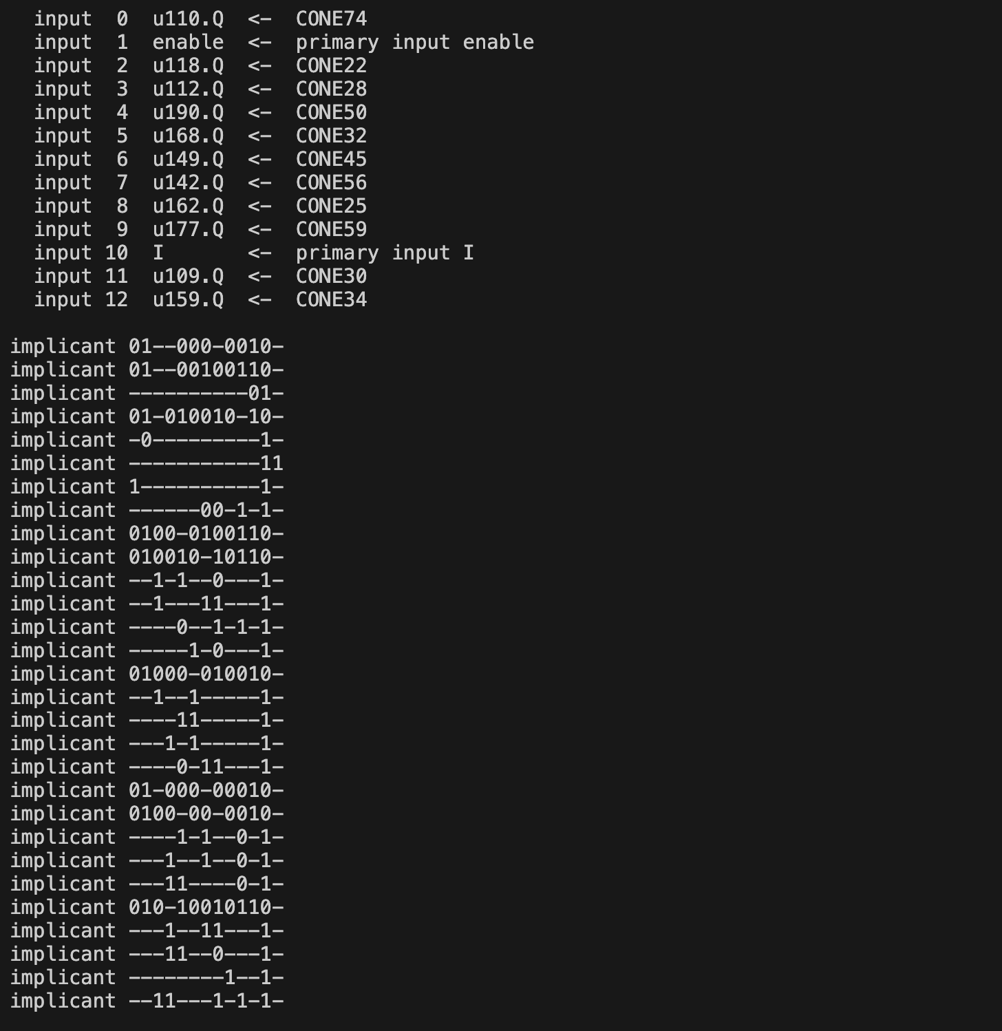
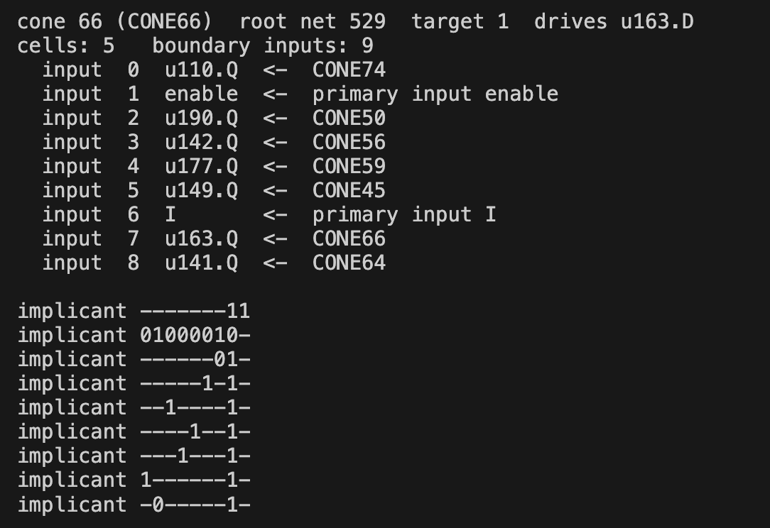
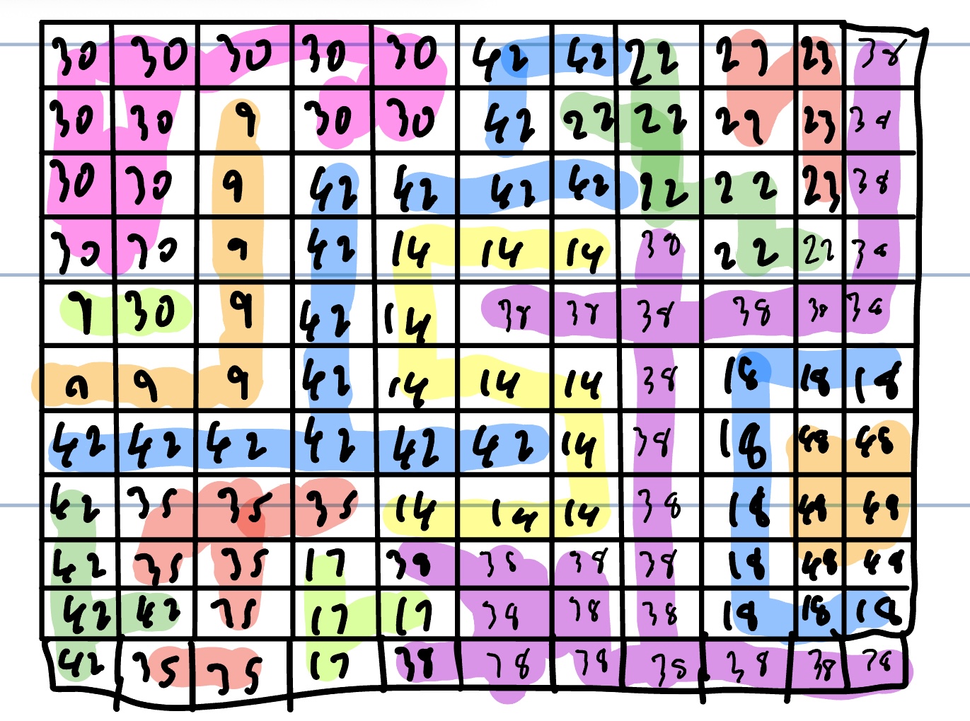
I wanted to add a section on a correction from my previous write-up. In "bit checking with control," I gave an example of decoding cone 30, which is actually wrong, as I wrote at the bottom. There were two things about the top group of cones in cone 98 that made me revisit the problem. Why did high signals around the specific point where it should go high also trigger the system of two cones? This checker is searching for a specific combination of 121 bits. Secondly, why was there, right below it, a structure that did the same thing but correctly? So I threw two cones into my z3 decomposeCone tool; the image of the output is shown below, and there's something very obvious. That middle section of bits is all control bits. For cone 66, the first example there is only one point in time, shown by the control bit, when that signal can be high. For cone 30, there are 4 distinct times it can be high. So I had to find out where these possible points were. Did they just represent things like what triggered cone 95? Or was it a pattern? I will show an example of how you can see which points on the 11x11 grid a 1 causes a high signal. This is a table deriving which 1s trigger cone 27(chosen because it is the smallest). The conclusion on the right now makes a lot more sense when you see all the control bits, and once those are specified, only specific cycles are left. To see all the derivations, you can see pages 17 and 18 of my notes during this puzzle.
| 74 | en | 22 | 28 | 32 | 45 | 50 | 56 | 25 | 59 | I | 27 | 29 | |
|---|---|---|---|---|---|---|---|---|---|---|---|---|---|
| 0 | 1 | 0 | - | 0 | 1 | 1 | 1 | 0 | 0 | 1 | 0 | - | col 8 cyc 0-11,22-33 |
| 0 | 1 | 0 | - | 0 | 1 | 1 | 1 | 0 | 0 | 1 | 0 | - | col 9 cyc 22-44 |
| 0 | 1 | 0 | - | 0 | 1 | 1 | 1 | 0 | 0 | 1 | 0 | - | col 7-8 cyc 22-33 |
| 0 | 1 | 0 | - | 0 | 1 | 1 | 1 | 0 | 0 | 1 | 0 | - | col 10 cyc 33-44 |